|

|
No.57 April, 2008 |
| |
Basic Science
New Way to Fabricate Carbon Nanotube Crystals
Two research groups separately headed by Sun Lianfeng, research fellow from the National Center for NanoScience and Technology (NCNST) China, and Xie Sishen, CAS member from the Institute of Physics (IOP), CAS have cooperated successfully to develop an effective fabrication of carbon nanotube crystal by taking advantage of their pervious achievement in the Large-Scale Synthesis of Rings of Bundled Single-Walled Carbon Nanotubes by Floating Chemical Vapor Deposition (Adv. Mater.18, 1817(2006)). Researchers have developed a low-cost and effective method to align single-walled carbon nanotubes (SWNTs) using a series of diamond wire drawing dies. The obtained SWNTs are highly dense and perfectly aligned. X-ray diffraction (XRD) that, although the diameters of SWNTs can not be controlled to an inch, the highly dense and perfectly aligned SWNTs (HDPA-SWNTs) with possibly the largest diameter can form a two-dimensional triangular lattice under the van der Waals�� force when there are appropriate growing conditions and the SWNTs�� diameter is shortened. They observe a sharp (002) reflection in the XRD pattern, which should be ascribed to an intertube spacing 3.39 ? of adjacent SWNTs. This peak corresponds to a d-spacing of 3.39 ?, which is usually found in graphite or multiwalled carbon nanotubes (d(002) ) 3.4 ?) and is believed to arise from the nearly ideal graphitic packing of SWNTs due to van der Waals interaction. Meanwhile, Raman spectra reveal that the radical breath mode (RBM) of SWNTs with larger diameter in the HDPA-SWNTs is notably suppressed compared with that of as-grown SWNTs. It shows that there are stronger interactions between SWNTs. The HDPA-SWNTs have a large density, -1.09 g/cm3, and a low resistivity, ��2 m�� cm, at room temperature, as well as a large response to light illumination.
Their work is of significance for the study over characteristics of carbon nanotube crystals (such as the superconductive property may emerge after the doping operation). The online version of the new achievement has been reported in the March 14 issue of Nano Letters.
New Step in Reconstruction of Si Semiconductor Research
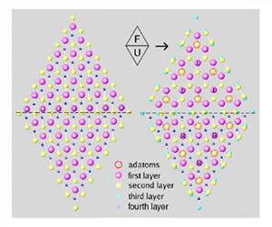
Researchers from the Institute of Physics (IOP), CAS have made a new progress in the reconstructed surface phase of Si(111)-7x7 and the corresponding phase dynamics. Their work was reported in the Feb. 8 issue of Physical Review Letters (100, 056103 (2008)).
On basis of the systematic analysis of massive experimental data, Research Fellow Liu Banggui and his doctorate student Xu Yechuan propose a natural two-speed model for the phase dynamics of this semiconductor phase transition to high-temperature unreconstructed phase. They formulate the phase dynamics by using phase-field method and adaptive mesh refinement technique. The simulated results show that a 7x7 island decays with two different rates �C the fast rate decay reflecting the changes of basic characteristics of the reconstructed surface phase and the slow rate one describing the subsequent atomic relaxation in a large size. These results are totally identical with the LEEM experiments, indicating the mode captures the essentials of this phase transition. This phase-field research produces satisfied results and the corresponding theory is a reliable approach to phase dynamics of surface phase transitions.

Progress in Intrinsic Spin Hall Effect Research
Based on the multiband effective-mass theory, Research Fellow Chang Kai and Doctorate Student Yang Wenji from the Institute of Semiconductor, CAS have discovered a strong nonlinear relationship of spin splitting against the growing of electron wave vector, when working over the spin track coupling of the narrow gap semiconductor quantum wells. The new model built by them well describes the nonlinear behavior and provides the physical image of nonlinear origin. Recently, they collaborated with Prof. Shou-Cheng Zhang from the Stanford University in USA in the research in the spin Hall effect of narrow gap semiconductor quantum wells. These researchers established a unified theoretic framework for spin Hall effect relating to n and p-typed semiconductors by adopting the Green��s function method and on the basis of the multiband effective-mass theory. The modification to the cone angle of impurity scattering has been also taken into consideration. The new theory can nicely deal with the strong conduction-valence band coupling narrow gap semiconductor quantum wells. By tuning the Cd content, the well width, or the bias electric field across the quantum well, the intrinsic spin Hall Effect can be switched on or off and tuned into resonance under experimentally accessible conditions. The switching on and off effect may be used to demonstrate the existence of the intrinsic spin Hall Effect. The series of new discoveries have been published by Physical Review Letters (PRL, 100, 056602(2008)) with the title ��Intrinsic Spin Hall Effect Induced by Quantum Phase Transitions in HgCdTe Quantum Wells��.
copyright © 1998-2010
CAS Newsletter Editorial Board: 52, Sanlihe Road, Beijing 100864,
CHINA
Email: slmi@cashq.ac.cn